Faculty of Electrical Engineering and Information Technology
JUN. PROF. DR. ANDREW R. GIBSON, FACULTY FOR ELECTRICAL ENGINEERING AND INFORMATION TECHNOLOGY
Research in the group is focused on the use of plasma-driven chemistry to enable novel technologies in the areas of biomedicine and sustainable chemical processing. To do this, methods to characterise and control the non-linear chemical processes in plasma sources are developed. Strong emphasis is placed on a combination of compu-tational and experimental measurements to obtain detailed insights into chemical pathways and enable comput-er-aided design of plasma sources for each application. The research programme includes; method development e.g. the construction of simulation frameworks , chemical reaction mechanisms and experimental protocols for reactive species measurement, such as absorption spectroscopy. These methods subsequently applied to under-stand the interaction of plasmas with application targets in the context of plasma-based disinfection processes, plasmas-based cancer therapy and chemical conversion in gases and liquids.
Keywords: plasma chemistry, biomedicine, sustainable chemical processing, disinfection, cancer therapy
Webpage: Biomedical applied plasma technology
FACULTY OF ELECTRICAL ENGINEERING AND INFORMATION TECHNOLOGY
DR. DENIS EREMIN, THEORETICAL ELECTRICAL ENGINEERING, DEPARTMENT OF ELECTRICAL ENGINEERING AND INFORMATION SCIENCES
Research is focused on the design, implementation, verification, validation, and application of novel numerical algorithms aimed at numerical modeling of various types of plasma discharges and on analysis of the resulting data. A particular emphasis is put on the multi-dimensional kinetic modeling of high-density plasmas operated at low pressures, which can be found in capacitively coupled, microwave-driven, dc- or rf-driven magnetron reac-tors, or Hall thrusters used in space propulsion. To make the corresponding simulations tractable, high-performance technologies based on the utilization of graphics-processing units (GPU), message-passing interface (MPI) or openMP are used. The simulation data obtained are analyzed and employed in the development of theo-retical understanding of the phenomena taking place in such plasmas.
Keywords: low temperature plasmas, magnetized plasmas, plasma modeling, algorithm development, high perfor-mance computing
Webpage: Theoretical Electrical Engineering
FACULTY OF ELECTRICAL ENGINEERING AND INFORMATION TECHNOLOGY
PROF. DR. MARTIN HOFFMANN, MICROSYSTEMS TECHNOLOGY
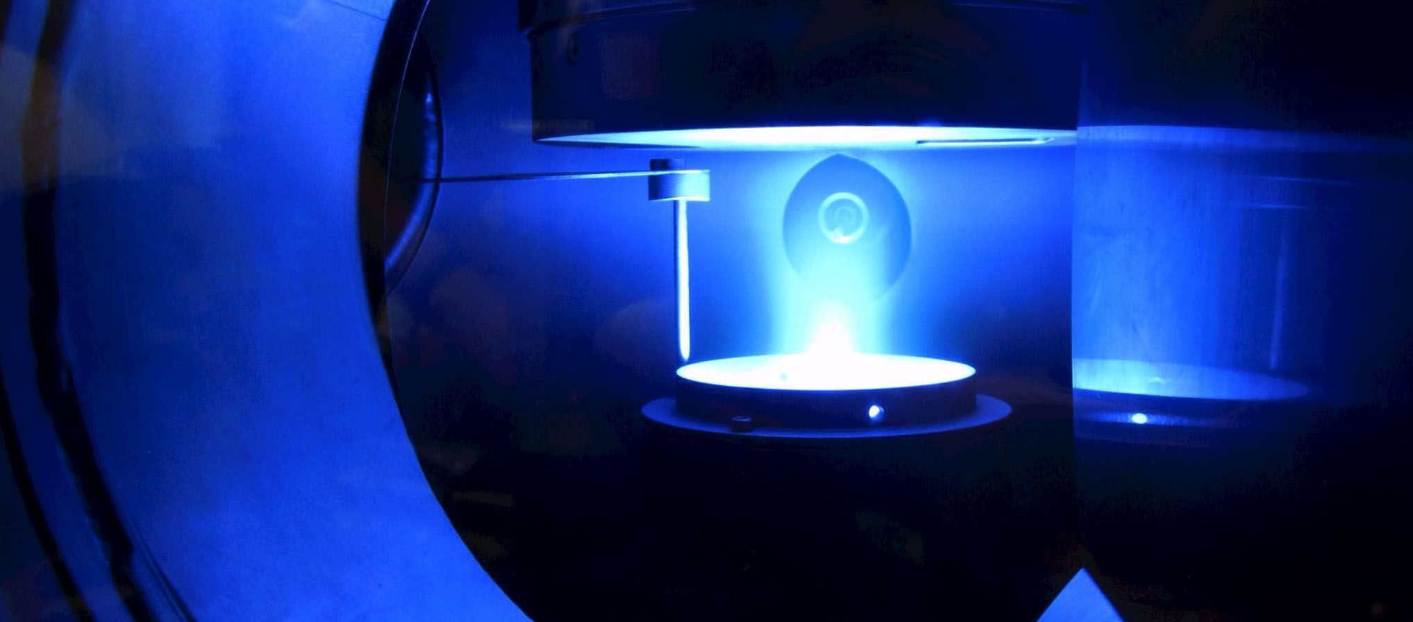
 The group uses different plasmas for deposition and etching of microsystems and microelectronics. It hosts the “Forschungslabor Mikroelektronik Bochum für 2D-Elektroniksysteme”, funded by BMBF within the ForLab initia-tive. The technological backbone are a three-chamber cluster tool for physical vapour deposition (PVD) and a five-chamber cluster tool for plasma-based CVD including atomic layer deposition (ALD) and reactive ion etching (RIE) / atomic layer etching (ALE). Both clusters are installed in 2021 and are open for research cooperation. The key research topics are microelectronics based on 2D-materials (new materials, selective etching of 2D-materials, process integration) and innovative microsystems in silicon and in glasses based on reactive ion etching. All pro-cesses are available on wafer scale (silicon and glass) up to 200 mm diameter.
Keywords: plasma deposition, plasma etching, electronic systems, microsystems
Webpage: Microsystem technology
Faculty of Physics and Astronomy
DR. KLAUS SCHERER, CHAIR OF THEORETICAL PHYSICS IV
Main interests in the group are a.) non-thermal distribution functions (regularized kappa distributions) and its connected moments, and b) the large scale modeling of astrospheres (including the heliosphere). The first topic requires a kinetic description based on the Vlasov/Maxwell system. The study of the second topic requires large scale magneto-hydrodynamic models (based on the Cronos code), including multi-fluid simulations.
The heliospheric models are based on in situ spacecraft data, while the modeling of astrospheres requires remote data. The former is needed to understand the physics of the heliosphere, while the latter will help to understand the physical environment around exoplanets.
Keywords: solar wind turbulence, large scale multifluid MHD simulations, regularized kappa distributions
Webpage: Theoretical Physics IV

Faculty of Electrical Engineering and Information technology
PROF. DR. THOMAS MUSSENBROCK, CHAIR OF APPLIED ELECTRODYNAMICS AND PLASMA TECHNOLOGY (AEPT)
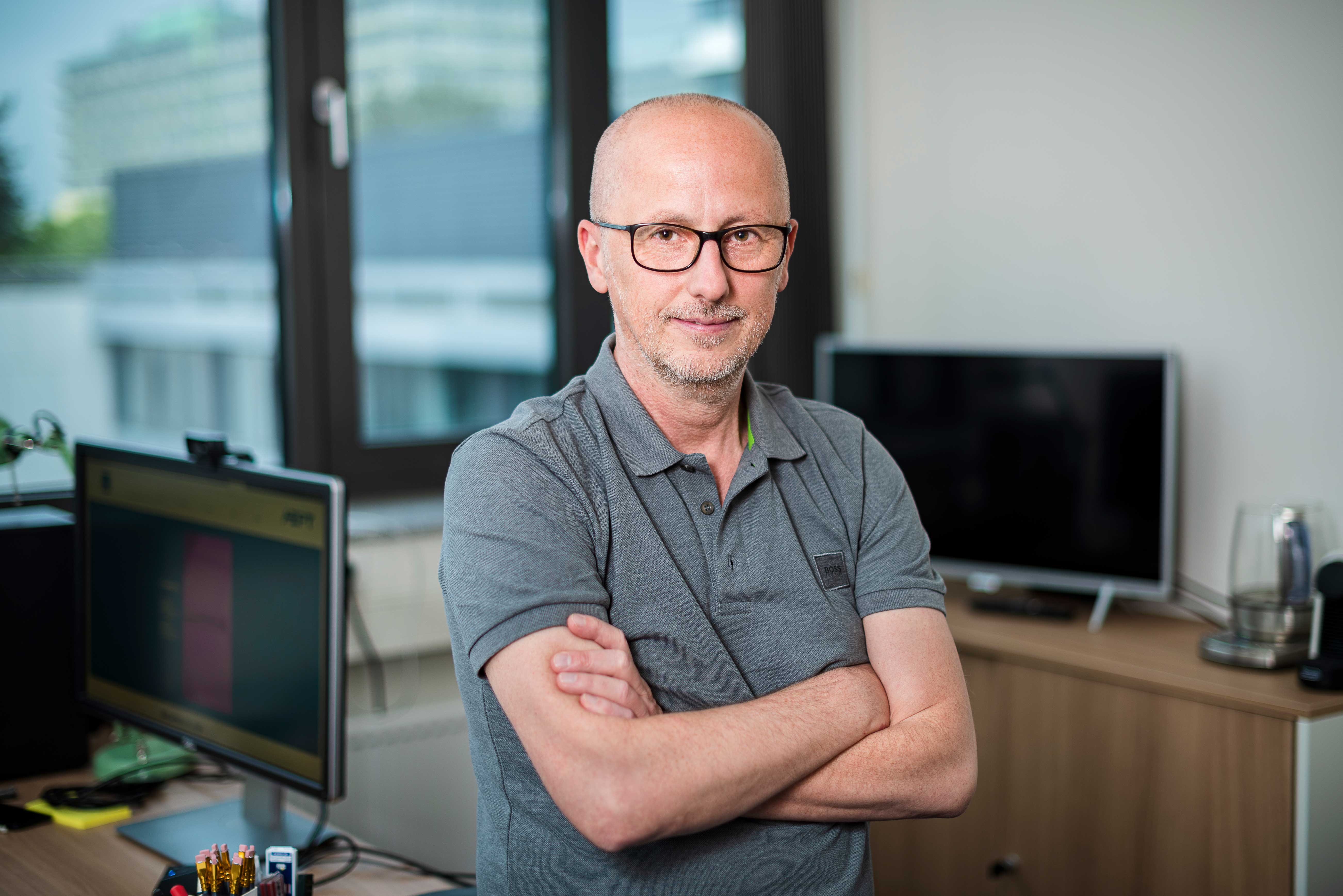
The research topics are in the area of low-temperature plasmas with the focus on materials processing. Thomas is also interest in the physics and application of nanoelectronic devices. Thomas and his team develop in analytical and numerical methods and tools for modeling and simulation of the aforementioned systems. The overall aim is to understand the macroscopic behavior of the systems based on the microscopic dynamics of the involved atoms, molecules, electrons and photons. In the framework of his research, he is member of the Collaborative Research Centres TRR 87 “Pulsed High-Power Plasmas for the Synthesis of Nanostructured Functional Layers”, CRC 1316 “Transient Atmospheric Plasmas – From Plasmas to Liquids to Solids”, and CRC 1461 “Neurotronics: Bio-Inspired Information Pathways”, all of which are funded by the German Research Foundation. Thomas is a trained electri-cian.
Keywords: Low-Temperature Plasmas, Plasma Processes, Modeling and Simulation, Nanoelectronic Devices
Webpage: Chair of Electrical Engineeringd and Plasma Technology
Faculty of Electrical Engineering and Information technology
PD DR. JULIAN SCHULZE, CHAIR OF ELECTRICAL ENGINEERING AND PLASMA TECH-NOLOGY
Dr. Schulze studies high frequency technological low temperature plasmas at low and high pressure, e.g. capaci-tively and inductively coupled discharges, based on experiments, simulations, and models. The primary research goal is to obtain fundamental insights into the plasma physics and chemistry to perform knowledge based plasma process development for e.g. plasma etching, sputtering, and deposition. Current externally funded projects range from electron heating in capacitive discharges, control of electron and ion energy distributions by Voltage Wave-form Tailoring, the Electrical Asymmetry Effect, plasma based control of radio frequency magnetron sputtering, multi-frequency sputter deposition of ceramics to dielectric plasma etching, streamer dynamics in dielectric barri-er discharges, and experimental validation of plasma simulations. These research activities are embedded in an international collaboration network including various academic institutions and companies.
Keywords: Technological High Frequency Plasmas, Plasma Surface Interactions, Plasma Diagnostics, Plasma Simula-tion, Knowledge based plasma process development
Webpage: Chair of Electrical Engineeringd and Plasma Technology
Faculty of Chemistry
PROF. DR. ANJANA DEVI, INORGANIC MATERIALS CHEMISTRY, FACULTY OF CHEMIS-TRY AND BIOCHEMISTRY
The research concept is based on bridging molecular chemistry and materials science to modulate materials prop-erties for functional devices. Current investigations focus on materials processing and tuning materials properties that are necessary to make new inroads into future technological developments. Large area fabrication of func-tional materials such as metals, oxides, sulfides, carbides and nitrides are targeted. The expertise lies in develop-ing novel precursors that are ultimately transformed into nanostructured thin films via chemical vapor deposition (CVD) and atomic layer deposition (ALD) processing. Plasma enhanced ALD is used as a powerful tool to fabricate gas sensors, passivation layers on electronic components, gas barrier layers on polymers, membranes for gas sepa-ration, 2D materials for electronics, gas sensors, energy storage etc.
Keywords: Plasma assisted atomic layer deposition, materials chemistry, 2D-Materials
Webpage: Bioinorganic Chemistry
