Prof. Dr. Martin Hoffmann, Microsystems Technology
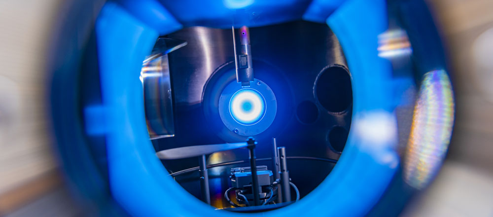
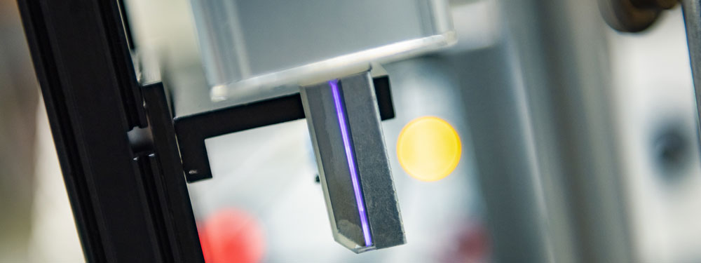
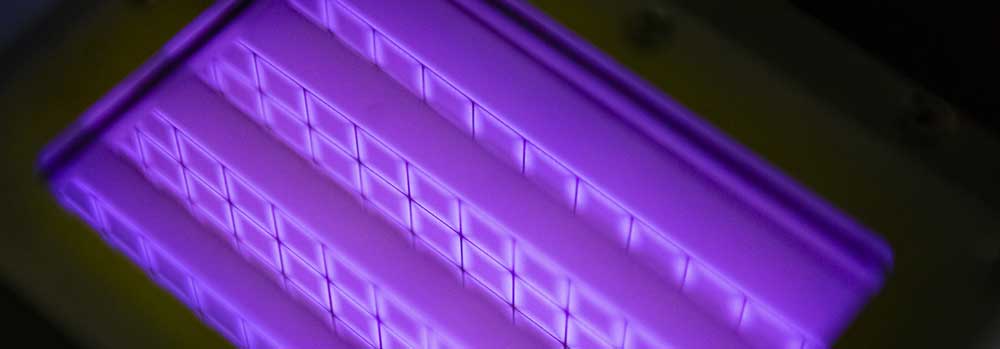
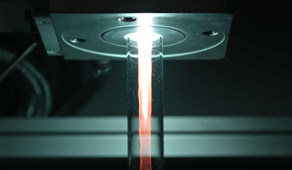
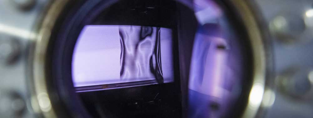
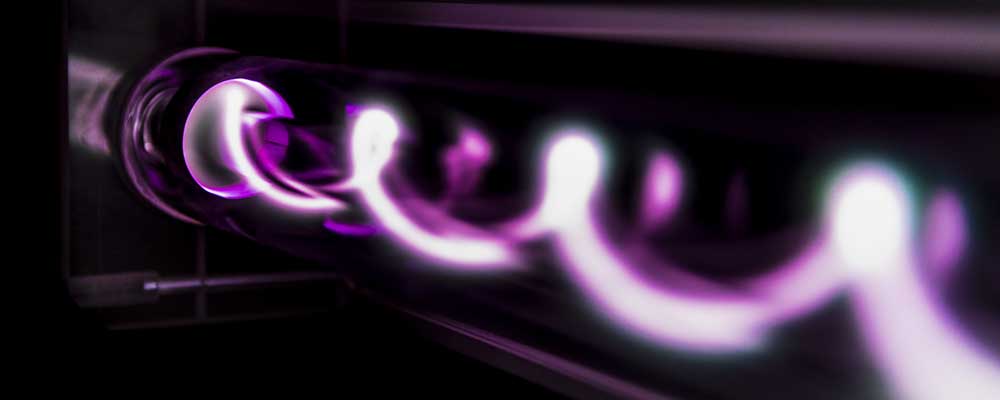
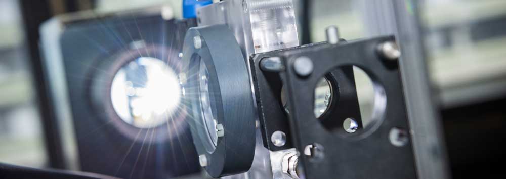
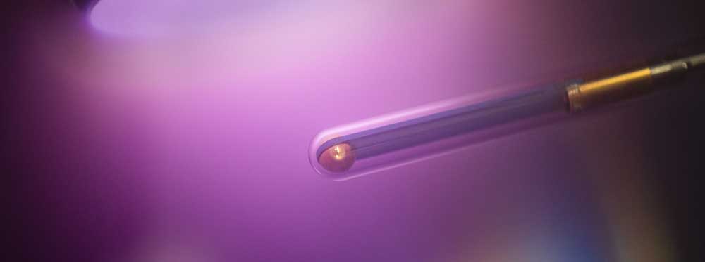
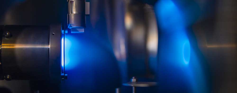
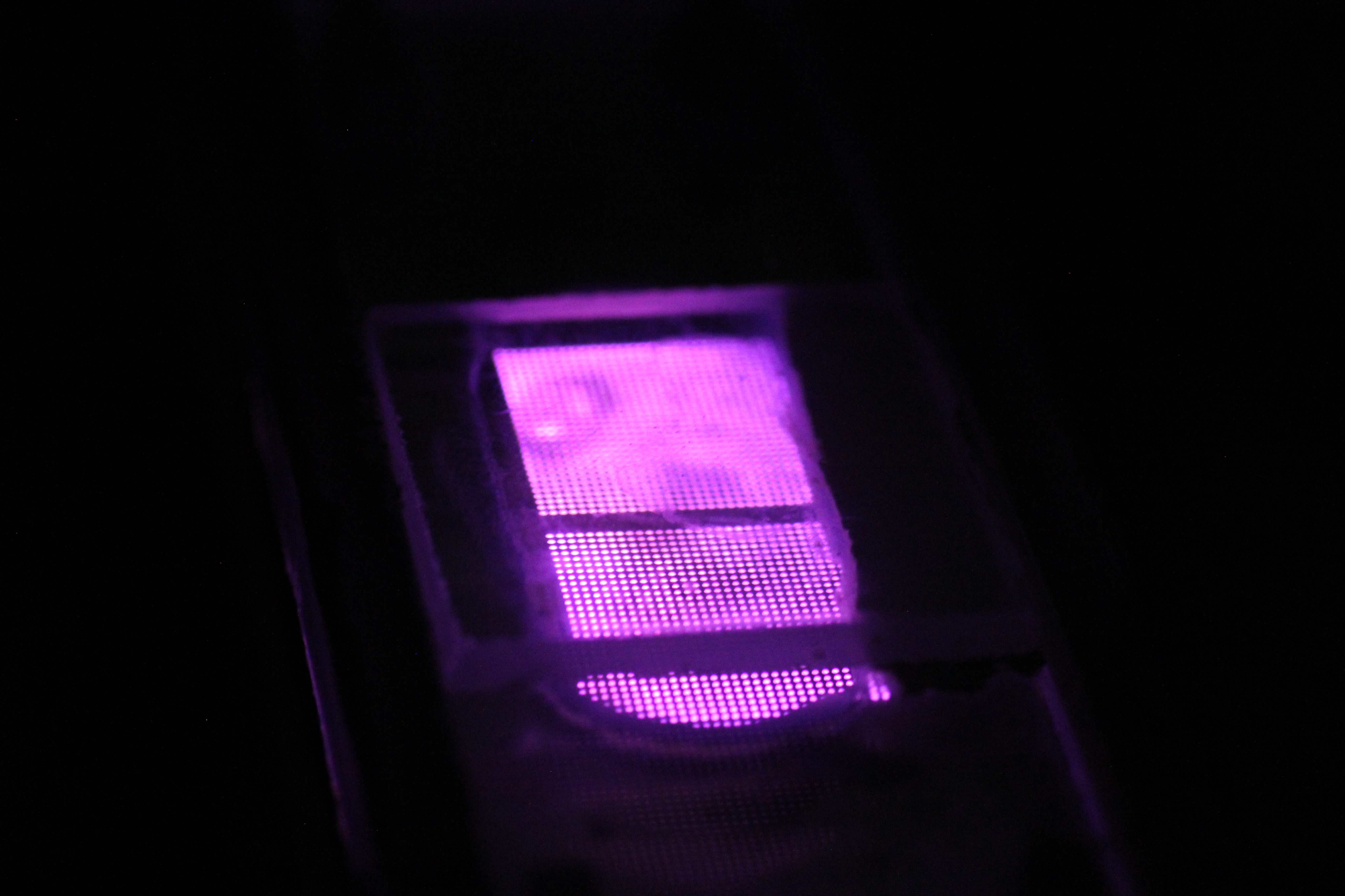
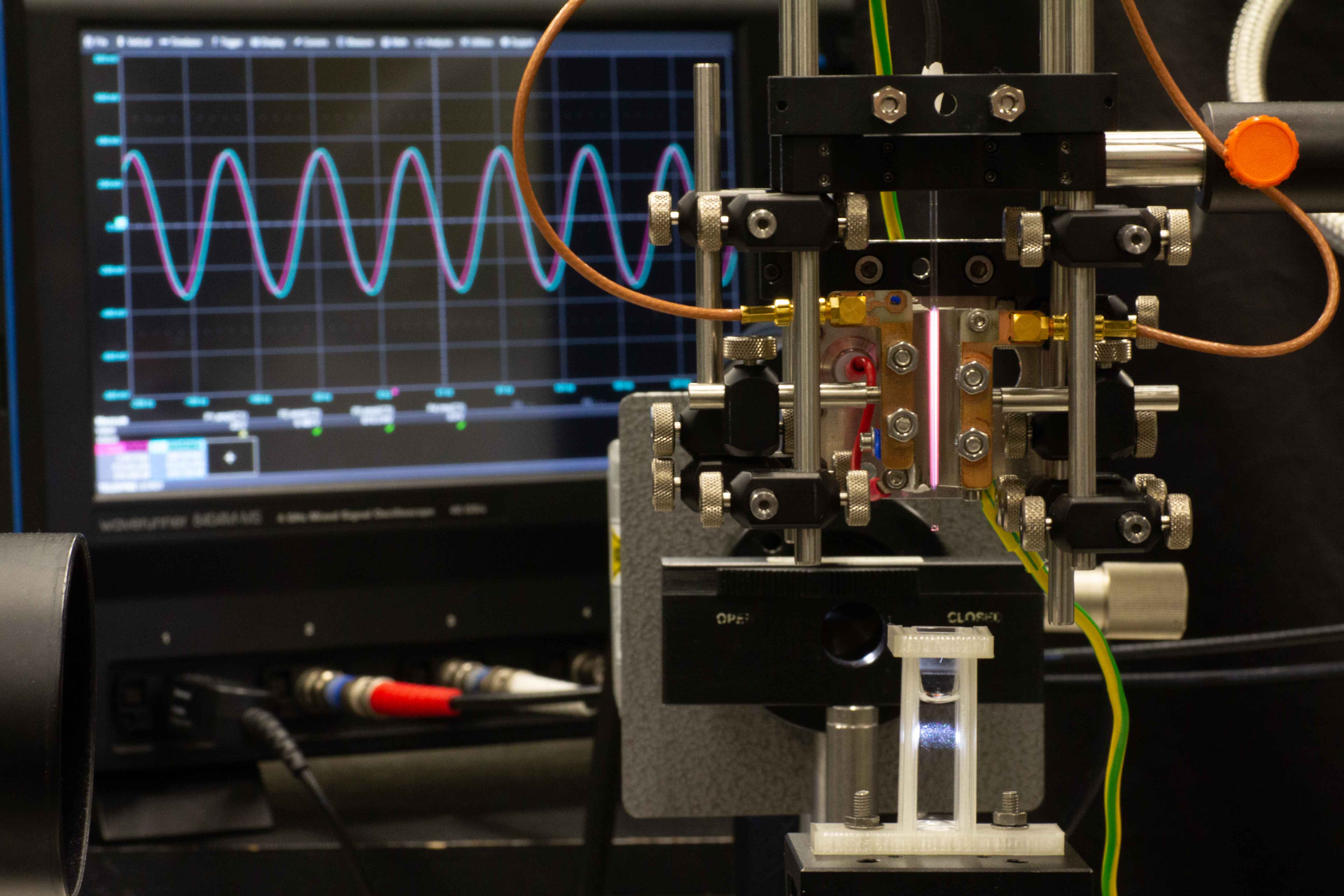
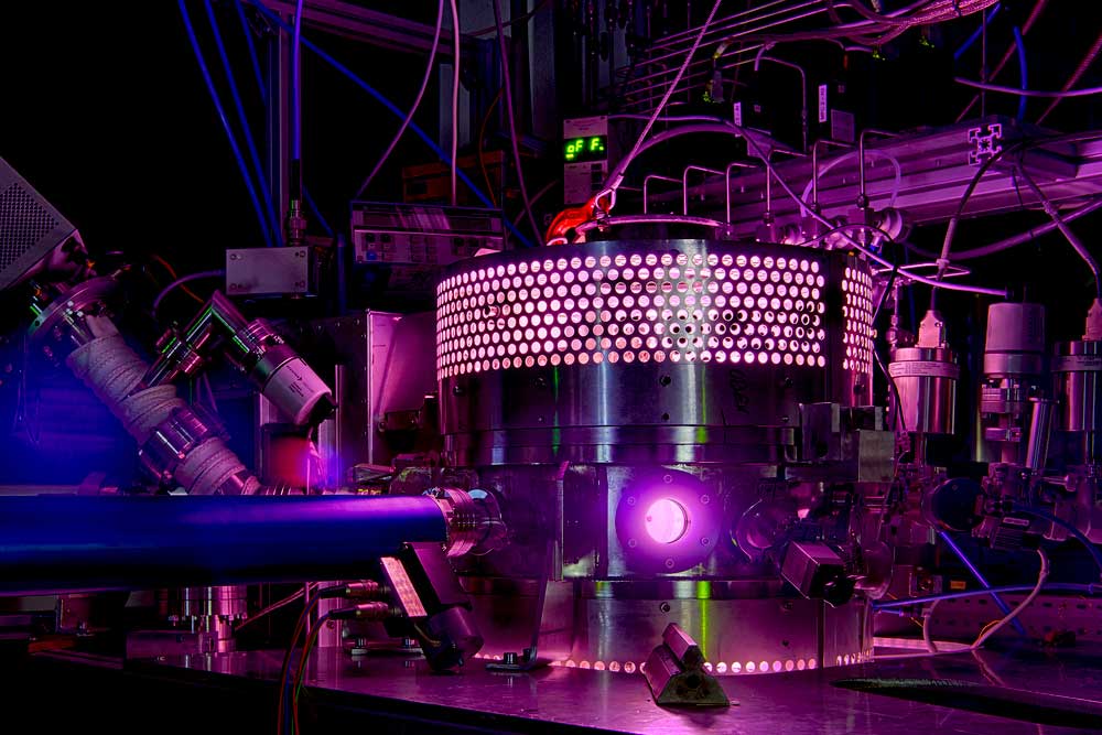
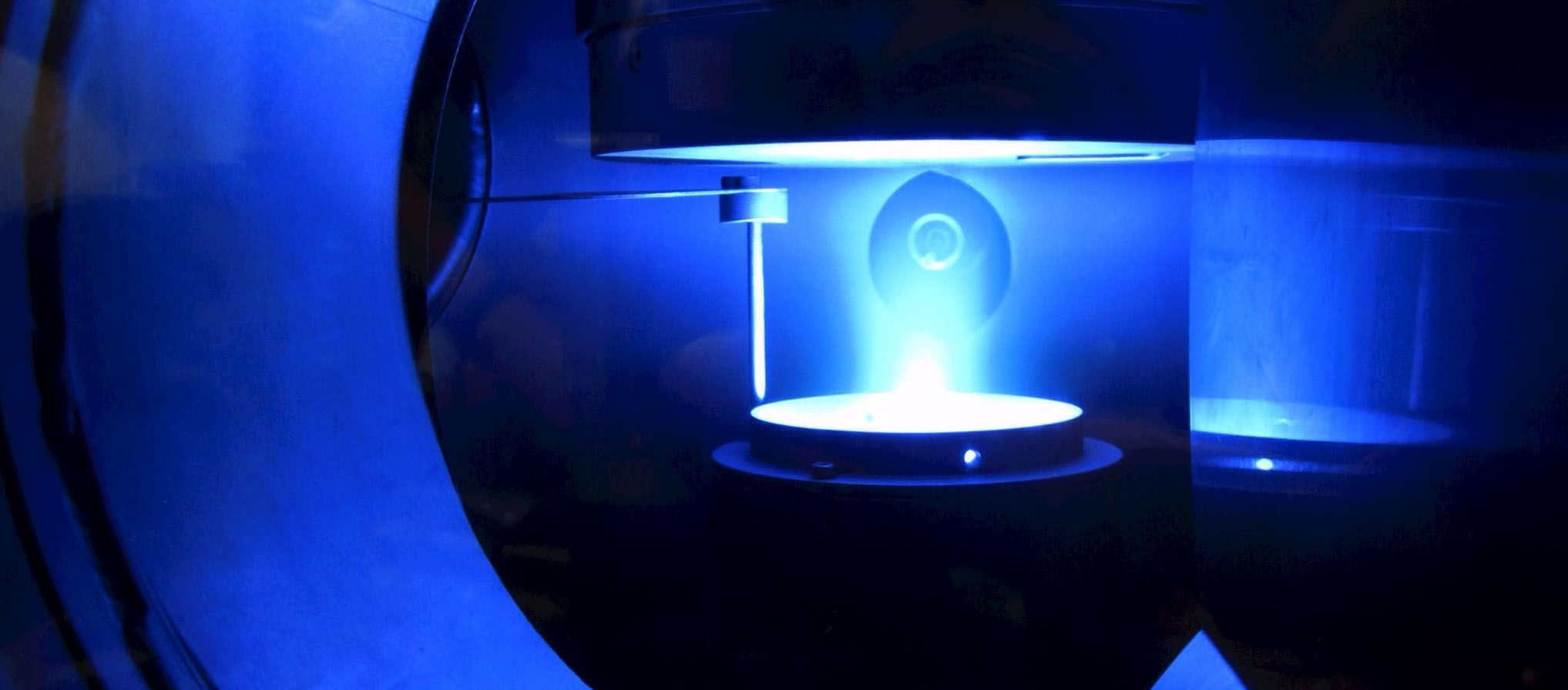
 The group uses different plasmas for deposition and etching of microsystems and microelectronics. It hosts the “Forschungslabor Mikroelektronik Bochum für 2D-Elektroniksysteme”, funded by BMBF within the ForLab initia-tive. The technological backbone are a three-chamber cluster tool for physical vapour deposition (PVD) and a five-chamber cluster tool for plasma-based CVD including atomic layer deposition (ALD) and reactive ion etching (RIE) / atomic layer etching (ALE). Both clusters are installed in 2021 and are open for research cooperation. The key research topics are microelectronics based on 2D-materials (new materials, selective etching of 2D-materials, process integration) and innovative microsystems in silicon and in glasses based on reactive ion etching. All pro-cesses are available on wafer scale (silicon and glass) up to 200 mm diameter.
Keywords: plasma deposition, plasma etching, electronic systems, microsystems
Webpage: Microsystem technology
ORCID: 0000-0001-9420-022X